by Gareth Parry, P.Eng
AISMALIBAR
Thermally conductive dielectrics used in the PCB substrate have been steadily growing in demand and application, with a surge following the development of LED lighting.
Many thermally conductive dielectrics are similar to the standard FR-4 dielectrics used in the PCB industry: epoxy (or polyimide) reinforced with woven glass with the addition of a conductive filler. The type, size, geometry, and concentration of the filler dictate the thermal/ mechanical properties of the dielectric. Typical conductivity values are 1.0–3.2 W/mK. In comparison, standard FR-4 has a thermal conductivity of 0.3W/mK, and copper is 398 W/mK.
Why the need for a thermally conductive dielectric?
The simple answer is thermal management of the system. Components mounted to the PCB or IMS need power to operate and the bi-product is thermal energy. Current running through a copper conductor will generate heat due the resistance of the copper. The greater the resistance, the more thermal energy that must be dissipated. As the temperature of the conductor increases, so does the resistance. In an uncontrolled design, one can experience a runaway condition where the increase in temperature drives an increase in resistance which drives an increase in temperature and so on, eventually destroying the circuit. In most situations this is not the case, but for high-power applications, and high-speed signals, thermal management is a real concern.
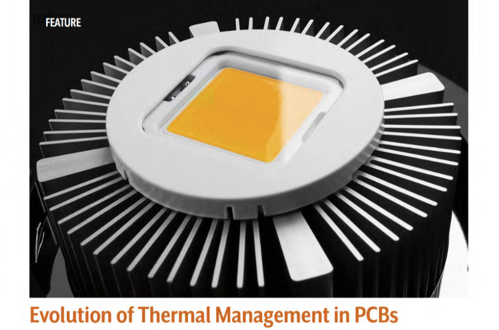
It is true that LEDs generally do not produce much heat, and are cool to the touch. Then why the exponential growth in demand for thermally conductive dielectrics? To put it in perspective, the energy consumed by a 100-watt incandescent bulb produces around 12% heat, 83% IR and only 5% visible light. The typical low watt LED might produce15% visible light and 85% heat[1]. But with high power LEDs (>1 watt), it is essential to remove the heat through efficient thermal management. Without good heat sinking, the internal temperature of the LED rises, and this will cause the LED characteristics to change.
As the junction temperature of an LED increases, the lumen (brightness) output decreases. The output wavelength also shifts with a change in junction temperature. The optimum way to address this heat passively is by using materials with a high thermal conductivity to move heat away from the junction as quickly as possible. The dielectric should have high thermal conductivity both laterally (x and y directions) as well as vertically through the base of the device.
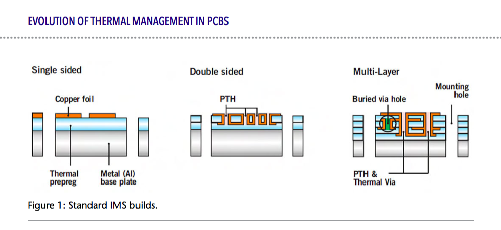
The circuitry routing for most LEDs is very simple, requiring only one layer of traces. A single-sided IMS would incorporate a thin thermally conductive dielectric sandwiched between a copper foil and aluminum heatsink. The dielectric helps to conduct the thermal energy away from the copper circuit to the aluminum heatsink where the energy is dissipated through convection to the air, or by conduction via a mechanical mounting system. More complex designs will have multiple layers of copper circuitry mounted to a heatsink. Components can be mounted on both sides by routing the aluminum prior to lamination. Very rarely will the aluminum heatsink be used as an electrical ground for the circuit. If electrical contact to the aluminum is a requirement for the design, it is a complex process to manufacture a plated via with connection to the aluminum. The aluminum interacts negatively to the electroless copper bath, and although feasible, few PCB shops offer the process. The easier approach is to use a copper heatsink versus aluminum.
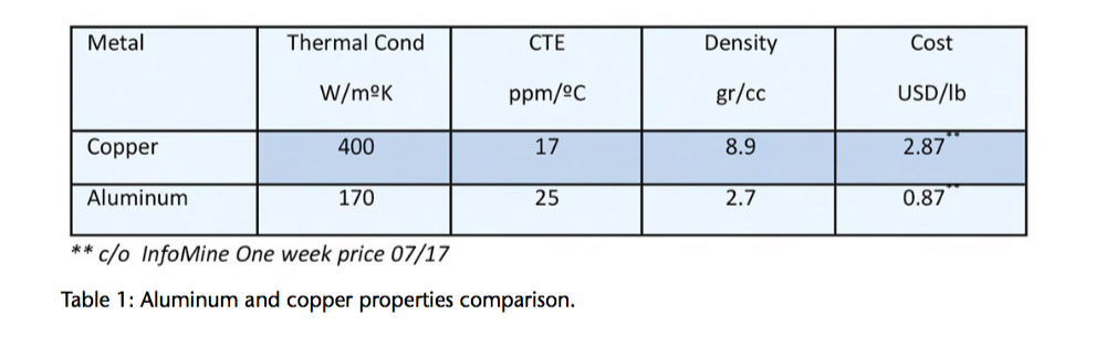
Copper is an exceptional thermal conductor (~400W/mK), but cost and weight considerations drive aluminum to be the preferred heatsink for most applications.
As discussed earlier, aluminum reacts negatively to electroless copper. This is also true with some surface finishes, for example, electroless nickel/immersion gold (ENIG).
There is an adverse reaction if the immersion gold bath is exposed to the aluminum. The work-around is to mask the exposed aluminum with a photo polymer and/or tape. Most fabricators do not want to take the risk of a scratch or pinhole in the protective material, and will avoid offering ENIG or ENEPIG as a viable surface finish for IMS product. Lead-free hot air leveling (HAL) is the most common finish, but the designer needs to verify their finish of choice with the fab house to be safe. The thermal conductivity of most laminates is reported as the thermal conductivity of the standalone dielectric. Some specification sheets report the thermal conductivity of the laminate (copper + dielectric + aluminum). This can be misleading. As an overall performance measure of the system, the designer may want to focus on the thermal impedance vs thermal conductivity. The thermal impedance (or thermal resistance) is the inverse of the thermal conductivity times the material thickness. Thus, the thinner the dielectric, the lower the thermal impedance. For the total system, or at a particular joint, the thermal impedance can be calculated (see equation 1).
One can see that the benefit from going from a 5-mil dielectric with 3.2 W/mK thermal conductivity, to a 1.5-mil dielectric with a thermal conductivity of 2 W/mK will have a 2x improvement in thermal impedance of the dielectric. The thinner the dielectric, the lower the thermal impedance. Dielectric withstanding voltage becomes a greater consideration as designs specify thinner dielectrics. To ensure quality and reliability, it is recommended that IMS laminate be 100% high pot tested by the laminate manufacturer prior to shipping. This will ensure there are no pinholes or foreign material in the thin laminate that could cause a high pot failure.
Traditionally, thermally conductive dielectrics have been used in PCB designs demanding high current loads. Motor controls, power supplies, AC/DC converters and solid-state relays were the major industry applications. As discussed, the LED industry has been the driving factor for the growth experienced over the last 10 years.
Recently, we have seen a growing interest for thermally conductive dielectric solutions in full build multilayer PCBs. The thermal energy output of components can be more effectively managed within the PCB versus use of expensive fans, heat pipes and liquid immersion cooling. In partnership with Advanced Micro Devices Graphic Card Division, Lazer-Tech PCB and Cartel Electronics, 6-layer and 12-layer, HDI, impedance-controlled PCBs were built using 2.2 W/mK and 3.2 W/mK thermally conductive dielectric systems throughout the stack. A 16% reduction in the thermal resistance was realized with the PCBs made with the thermally conductive dielectric as compared to the PCBs made with FR-4. This improvement in thermal impedance allows tremendous opportunities in cost savings long term.
Much more work is needed to fully appreciate the benefits of these materials in full build complex PCBs. As technologies continue to evolve the need for thermal management solutions in PCB design are only going to increase. PCB
Reference
1. Fact or Fiction: LEDs don’t produce heat, Tim Whitaker, LEDs Magazine.
by Gareth Parry, P.Eng
AISMALIBAR