Traditional coating processes for solder mask1 handle thickness as a single parameter for the whole board. There will be differences between the amount of material on the laminate or on the copper, and these will depend on the height of the copper and in some cases on the section of the copper feature. Overall, it is reproducible: It looks homogeneously green and it is easy to estimate the amount of material consumption. Therefore, everybody is happy.
Still, the homogenous colour stems from the presence of opaque fillers which, already in small quantities, would reduce the dependence of transparency on the coating thickness. In other words, with a top view, there is little clue left as to how thick the solder mask actually is. Cross sections are therefore a nice ally: In one sample, the geometrical details of copper, laminate (together with its many layers), and solder mask are in clear sight.
The predictability of the material consumption does not imply that the coating thickness benefits itself from the level of certainty: a ±20% variation on material consumption is solved with a temporary bigger stock space and might even be insignificant compared to bill-to-book fluctuations. Instead, the same variation on the solder mask thickness could bring about troubles in the PCB assembly because of poor predictability of the board topography.
Inkjet solder mask coating, in this early adoption phase, is evaluated by mimicking traditional solder mask. Furthermore, it could not be any different since the same CAM procedures define it on the printer tool. However, when removing this constraint, and by picturing CAM protocols that include the detail of solder mask thickness and other manufacturing details, several opportunities arise.
Before listing such opportunities, a brief description of how thickness is tunable: High DPI values allow an easy coalescence of drops. Dithering, as a means to reduced coverage, finely tune the amount of material and achieve the thickness specification.
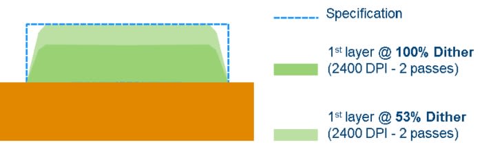
Figure 1: Thickness specifications and an example of how a hypothetical printhead with 1200 NPI can create it.
A trace for radio frequency (RF) signals delivers a signal fidelity depending on its geometrical and electrical parameters. The solder mask also takes part in this dependence as coating. The task of designers is to control RF performances through smart design. Sophisticated software packages support the designers by modelling various situations. A coated single trace is the simplest example; there the variation of solder mask thickness is a second order effect on impedance. With more complex structures, like differential traces, structures on a single layer (trace + ground), or edge-coupled traces2; any variation of the coating becomes more critical.
Still, no matter what final performances the model simulates, variations that shift from the simulated design will result in batch-to-batch fluctuation, or in the worst case, yield loss. Here is where the accurate control of thickness of inkjet is helpful. Finally, avoiding solder mask altogether is a good practice on an RF circuit. With traditional solder mask, this means placing the solder mask and then removing it, which in itself can turn into a cleaning accuracy debate. With inkjet, solder mask was never there in the first place. Therefore, whatever post-treatment maximizes RF performance, it will prefer the untainted surface left after the inkjet process.
A power circuit benefits from thick copper traces and high voltages to minimize heat loss. However, this leads to very thick solder mask layers, which are difficult to cure uniformly through their thickness. The variation on curing level of solder mask3 can result in failure due to ionic transfer in solder mask layers and the consequent conductive material creeping. For inkjet, even thicker layers would get, per unit of thickness, the same amount of curing. Thanks to layering, each thickness, even a few hundreds of micrometers, becomes a matter of layer stacking and after each layer, the solder mask is pinned. Consecutive pinning cumulates to a complete curing of the lowest layers.
Finally, yet importantly, here are some of the assembly concerns:Tombstones caused by thick solder mask
BGA bridging due to the “safe choice” of NSMD When thickness design becomes standard, the next level of CAM will see the components themselves define the topography of the solder mask. A fully integrated, high yield CAM.
CONTACT US TO LEARN MORE ABOUT SUSS PRODUCTS