Next-Generation Precision for High-Reliability Microvias
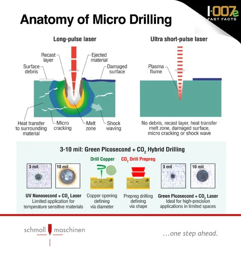
In today’s HDI and IC-substrate production environments, precision and consistency are no longer optional—they're essential. Traditional UV nanosecond laser systems have served the industry well, but as design rules shrink and reliability requirements grow, their limitations are becoming increasingly clear. Schmoll Maschinen GmbH has developed an advanced picosecond laser platform that overcomes the thermal and mechanical constraints of earlier-generation systems. By integrating picosecond pulses with beam shaping technology, Schmoll delivers a solution engineered for high-density PCB manufacturing and next-generation packaging.
Key technical advantages include:
- Overhang-free vias and clean ablation profiles that minimize post-processing
- Ultra-low taper angles, critical for stacked via integrity in multilayer designs
- Reduced heat-affected zones (HAZ) that protect surrounding dielectric and copper layers
- High-aspect-ratio via formation in materials down to 3 mils and below
This technology enables more reliable, high-yield drilling of microvias for complex HDI builds, including IC-substrates, flex-rigid hybrids, and advanced packaging formats. The result is improved electrical performance, tighter tolerance control, and longer-term product reliability—exactly what the market demands from cutting-edge PCB fabrication. To learn more about the science behind Schmoll’s laser drilling breakthroughs, check out the I-Connect007 interview with Dr. Stefan Rung: 👉 Read the article